AI-Based Semiconductor Defect Detection Using Edge Computing and Computer Vision
Abstract Semiconductor manufacturing demands extremely precise inspection because tiny defects can greatly impact the performance, reliability, and yield of chips. Traditional inspection methods often rely on rule-based image processing, manual checks, or centralized computing, which can struggle to handle the growing volume and complexity of high-resolution images. This paper introduces an AI-powered approach to detect defects in semiconductor wafers by combining computer vision, deep learning, and edge computing. Using a lightweight neural network running directly on edge devices, the system processes and analyzes inspection images locally. It can identify and classify various defect types like particles, scratches, pattern issues, cracks, bridging, and missing structures. By handling the data on-site instead of sending large images to a central server, the system reduces delays, bandwidth needs, and dependency on network reliability. Designed for near-real-time use in manufacturing, this approach aims to deliver fast, accurate defect detection while efficiently using computing resources. We evaluate the system’s performance with metrics such as accuracy, precision, recall, F1-score, and inference speed. Overall, this research shows how combining AI with edge computing offers a scalable and responsive solution to improve semiconductor defect inspection. Keywords: Semiconductor Manufacturing, Defect Detection, Artificial Intelligence, Computer Vision, Edge Computing, Deep Learning, CNN, Wafer Inspection, Machine Vision, Industrial AI.
1. Introduction
Semiconductors are at the heart of almost every modern electronic device—from smartphones and computers to cars, medical equipment, communication tools, and industrial machines. As semiconductor technology evolves, with smaller and more complex designs, the need for highly precise inspection during manufacturing becomes even more critical.
During the manufacturing process, a semiconductor wafer goes through many steps like deposition, lithography, etching, cleaning, implantation, and packaging. Defects can sneak in at any stage, lowering the number of usable wafers and impacting the reliability of the final product. That’s why catching these defects early is so important to ensure quality.
Traditional inspection methods rely on automated optical systems, scanning electron microscopes, image processing, and carefully crafted rules. While these methods have worked well, the growing complexity and shrinking size of defects present new challenges. Recent studies categorize defect detection techniques into three groups: image-processing-based, machine-learning-based, and deep-learning-based methods.
Artificial intelligence offers a promising alternative by teaching models to recognize defect patterns directly from the images. Deep learning methods, like convolutional neural networks (CNNs), can automatically learn what defects look like, helping to spot problems more accurately. Researchers have successfully applied models such as CNNs, Mask R-CNN, and CenterNet for defect detection in semiconductors.
However, many AI systems today rely on sending inspection images to cloud servers for processing. Since these images are often very large and numerous, this approach can be costly and slow due to the time and bandwidth needed for data transfer.
Edge computing tackles this issue by bringing AI processing closer to the source—the inspection equipment itself. By running trained models on local edge devices near the cameras, images can be analyzed immediately on-site. Only the key information, like defect type, location, and confidence scores, needs to be sent to the central system, saving time and reducing network load.
Building on this idea, our research proposes a smart, AI-driven semiconductor defect detection system that combines computer vision with edge computing to deliver fast, efficient, and accurate inspections.
2.Problem Statement
In semiconductor manufacturing, detecting tiny defects quickly and accurately is crucial. However, current inspection methods face several hurdles:
- Manual inspections take a lot of time and can be prone to mistakes.
- Traditional rule-based computer vision systems often struggle with the complex and ever-changing defect patterns.
- High-resolution inspections produce massive amounts of image data to process.
- Sending all this data to the cloud can cause delays and uses a lot of bandwidth.
- Deep learning models often need powerful computing resources, which may not always be available.
- There are often limited labeled images of defects to train AI models effectively.
- Changes in lighting, imaging setups, wafer designs, and manufacturing steps can make AI models less reliable.
Recent studies have shown that while AI performs well in labs, very few solutions are fully deployed in large-scale manufacturing. This points to ongoing challenges in making these systems robust and practical for real-world use.
3.Objectives
The goal of this research is to build an AI-powered semiconductor defect detection system that runs efficiently on edge computing devices, close to the inspection equipment.
Specifically, we aim to:
- Create a computer vision workflow tailored for semiconductor wafer images.
- Automatically detect common defect types.
- Train a deep learning model to classify or locate defects.
- Optimize the model so it can run smoothly on edge devices.
- Enable local image processing without constantly sending data to the cloud.
- Cut down the time it takes to detect defects.
- Measure detection performance using common accuracy and speed metrics.
- Compare how well edge-based detection performs against traditional cloud-based methods.
- Explore the practicality of using lightweight AI models in semiconductor manufacturing environments.
This approach hopes to make defect detection faster, more accurate, and more adaptable to real production lines.
4. Research Questions
This research investigates the following questions:
RQ1: Can deep-learning-based computer vision accurately detect semiconductor wafer defects?
RQ2: Can a lightweight AI model provide sufficiently high detection performance on an edge computing device?
RQ3: How much can edge computing reduce inference latency and network dependency compared with cloud-based processing?
RQ4: Which preprocessing and model-optimization techniques provide the best balance between accuracy and computational efficiency?
RQ5: Can the proposed system support near-real-time semiconductor inspection?
5. Literature Review
5.1 Traditional Semiconductor Defect Inspection
Traditional methods for inspecting semiconductor defects have mainly relied on optical inspection, image processing, statistical analysis, and electron microscopy. These techniques are still important because defects often occur at incredibly small scales.
Classic computer vision techniques used in this area include:
· Thresholding
· Edge detection
· Morphological operations
· Template matching
· Image subtraction
· Blob detection
· Texture analysis
· Statistical pattern analysis
However, these manually designed features sometimes struggle to adapt well to the wide variety of semiconductor structures and defect types that exist.
5.2 Machine Learning for Defect Detection
Machine learning has helped improve defect inspection by teaching systems to recognize patterns from labeled images. Traditional classifiers like support vector machines, random forests, and nearest neighbor algorithms have been explored for industrial use.
Still, semiconductor manufacturing involves very complex visual patterns, and as defects become smaller, simpler methods like thresholding often fall short. That’s why recent research has been focusing more on deep learning techniques to automate defect inspection.
5.3 Deep Learning and Computer Vision
Deep learning models excel because they can automatically learn multiple layers of features from inspection images.
Convolutional neural networks (CNNs) are especially powerful since their convolution layers can detect things like:
· Edges
· Textures
· Shapes
· Irregular patterns
· Local structural abnormalities
Beyond just spotting if defects are present, object-detection models can also pinpoint exactly where defects appear in an image.
For example, a model called SEMI-CenterNet customized the CenterNet architecture specifically to locate and classify defects in semiconductors while improving speed and efficiency.
Another popular model, Mask R-CNN, has been used for detecting and segmenting semiconductor defects, which helps not only identify defects but also measure their precise size.
More recently, diffusion-based methods have started to be explored for both classifying and segmenting defects in semiconductor images.
This growing toolbox of AI techniques shows promising advances in making semiconductor defect inspection faster, more accurate, and more adaptable.
6. Proposed Methodology
The system we propose follows six main steps:
Image Acquisition → Preprocessing → AI Detection → Edge Inference → Defect Classification → Result Transmission
6.1 Image Acquisition
Images of semiconductor wafers can be captured using various tools such as:
· Industrial cameras
· Optical microscopes
· Automated optical inspection systems
· Scanning electron microscopes
For student projects or smaller-scale implementations, publicly available datasets of semiconductor wafer defects can be used instead of capturing new images.
6.2 Image Preprocessing
Before feeding images into the AI system, they need to be preprocessed to make sure they are clear and consistent for analysis.
This preprocessing might involve:
· Resizing images to a standard size
· Removing noise or unwanted artifacts
· Enhancing contrast to highlight important features
· Normalizing the image data for better AI performance
· Sharpening details to make defects more visible
· Extracting specific regions of interest where defects are likely
· Applying data augmentation techniques to expand the training dataset
Data augmentation can include:
· Rotating images
· Flipping them horizontally or vertically
· Scaling or cropping parts of the image
· Adjusting brightness and contrast
These steps help make the AI model more robust, especially when there isn’t a large amount of training data available.
7. AI Model
For this system, we use a lightweight convolutional neural network (CNN) or an object-detection model that’s designed to work efficiently on edge devices.
Some options include:
- MobileNet
- EfficientNet
- YOLO (You Only Look Once)
- SSD (Single Shot Detector)
- EfficientDet
- Custom lightweight CNNs
Since the goal is not just accuracy but also quick processing and low power use, lightweight models like YOLO or MobileNet are great choices for edge computing.
The model takes an image of a semiconductor wafer and outputs:
- The location of any detected defects
- The type or class of each defect
- A confidence score showing how sure the model is
- The total number of defects found
For example, the model might classify defects as:
| Defect Type | Classification |
| Scratch | Defective |
| Particle | Defective |
| Crack | Defective |
| Bridge | Defective |
| Missing Pattern | Defective |
| Normal Wafer | Non-defective |
Table.7.1
This allows the system to quickly and accurately identify problem areas on wafers during manufacturing.
8. Edge Computing Architecture
In our proposed setup, the AI system that detects defects works right next to the semiconductor inspection equipment, rather than relying on distant servers.
Here’s how the system flows:
· The semiconductor wafer is first captured by an industrial camera.
· The images then go through preprocessing to get them ready for analysis.
· These preprocessed images are sent to an edge AI device—a small, powerful computer located close to the inspection point.
· The edge device runs a lightweight CNN or YOLO model to quickly analyze the image.
· Based on the analysis, the system decides if a defect is detected or if the image is normal.
· If a defect is found, it gets classified, and this information is saved to a local database.
· The results then feed into the manufacturing monitoring system to help track wafer quality in real time.
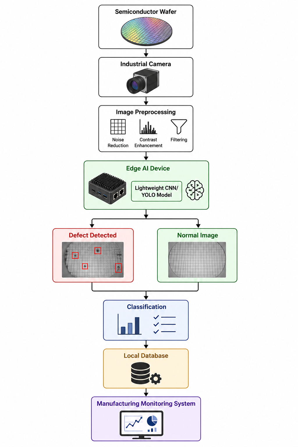
Figure.8.1
Instead of sending large raw images over the network, the edge device only uploads important data like:
· Defect type
· Confidence level of detection
· Exact location of the defect
· Time the inspection was done
· Identification details of the wafer
· Selected images of the defects
This approach reduces delays, lowers bandwidth use, and keeps the system running smoothly even if the network connection is unstable.
9. Edge Device Selection
To run the AI system close to the inspection equipment, we can use edge AI platforms like:
- NVIDIA Jetson Nano
- NVIDIA Jetson Orin Nano
- Raspberry Pi paired with an AI accelerator
- Intel-based edge computers
- Google Coral TPU
For student projects or prototypes, the NVIDIA Jetson platforms are a great fit because they support GPU acceleration, which speeds up deep learning tasks.
To make the model run efficiently on these devices, we can apply optimization techniques such as:
- Quantization (reducing model size)
- Pruning (removing unnecessary parts)
- Knowledge distillation (transferring knowledge from a large model to a smaller one)
- Using lower resolution images
- TensorRT optimization (a tool for faster inference on NVIDIA devices)
These methods help reduce memory use and speed up processing, while still keeping accuracy at a good level.
10. Model Training
We split the dataset into three parts:
- 70% for training the model
- 15% for validating and tuning the model’s settings
- 15% for testing its final performance
The typical training process looks like this:
11. Performance Evaluation
To truly understand how well the system works, we need to look beyond just accuracy and use several key metrics:
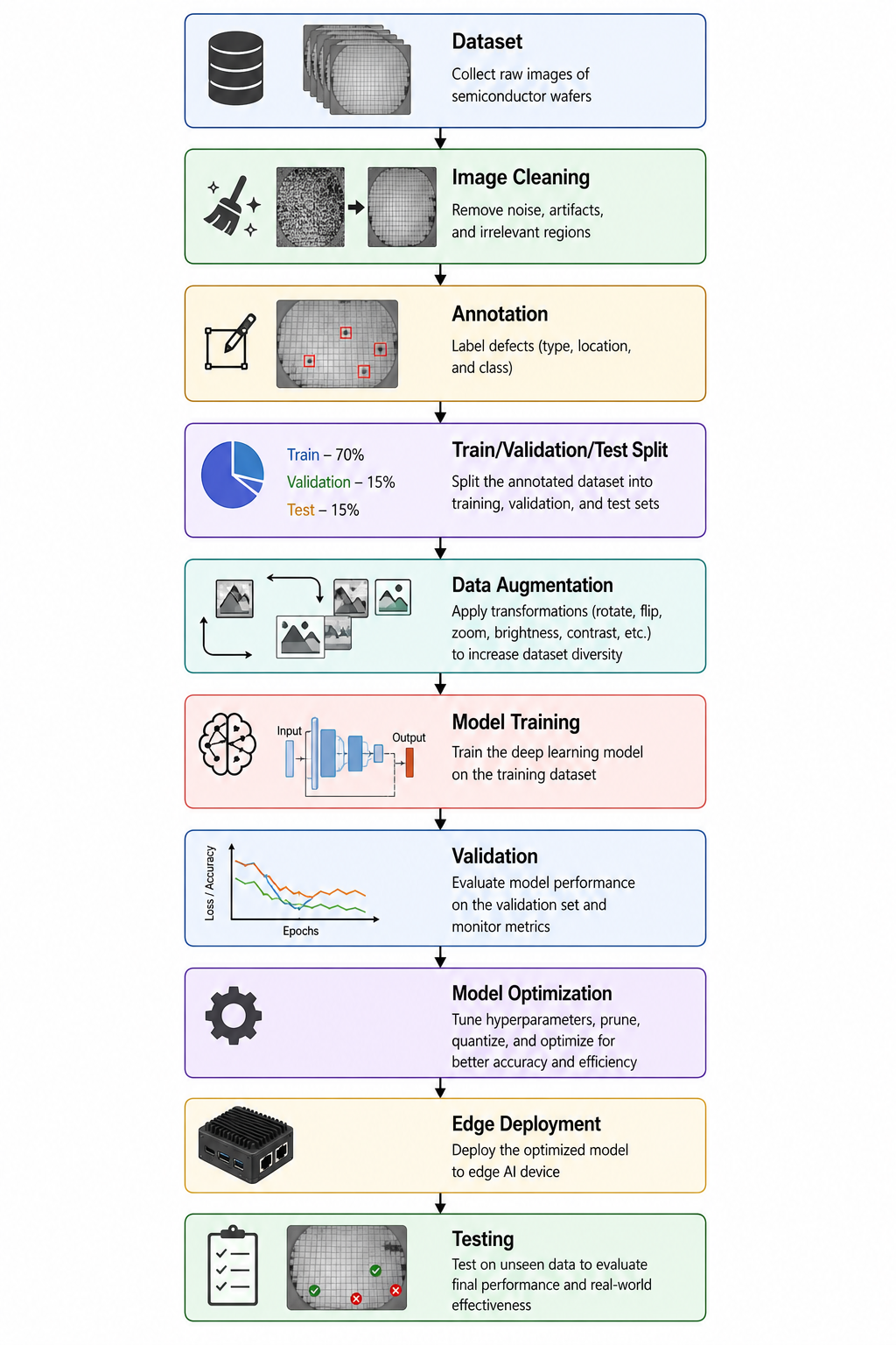
Figure.11.1
11.1.Accuracy
This measures the overall percentage of correctly identified samples, both defects and non-defects.
where:
- TP = True Positives (correctly detected defects)
- TN = True Negatives (correctly identified non-defects)
- FP = False Positives (false alarms)
- FN = False Negatives (missed defects)
11.2.Precision
Precision tells us how many of the detected defects are actually true defects. High precision means fewer false alarms.
11.3.Recall
Recall shows how many real defects the system successfully caught. In semiconductor manufacturing, high recall is crucial because missing defects can hurt product quality.
11.4.F1-Score
This combines precision and recall into one number, balancing both.
11.5. Mean Average Precision (mAP)
For object-detection models, mAP measures how well the system detects defects across different types and how accurately it pinpoints their location.
11.6. Inference Latency
Since this system runs on edge devices, it’s important to measure how long it takes to process each image. Lower latency means faster inspections.
Using these metrics ensures we get a complete picture of the system’s accuracy, reliability, and speed in real-world semiconductor inspections.
12. Expected Results
We expect the proposed system to deliver:
- Automated detection of semiconductor defects
- High accuracy in classifying and locating defects
- Faster detection with reduced processing delays (low inference latency)
- Less reliance on cloud computing
- Lower network bandwidth usage
- Quicker responses to manufacturing defects
- The ability to support continuous, real-time inspection in line with production
- Improved scalability for growing semiconductor manufacturing needs
Actual numbers for performance metrics will come from running the model on real datasets and should not be guessed beforehand.
A sample results table might look like this:
| Metric | Cloud AI | Edge AI |
| Accuracy | TBD | TBD |
| Precision | TBD | TBD |
| Recall | TBD | TBD |
| F1-score | TBD | TBD |
| mAP | TBD | TBD |
| Inference Time | TBD | TBD |
| Memory Usage | TBD | TBD |
Table.12.1
13. Advantages of the Proposed System
- Low Latency: Processing happens close to the inspection equipment, cutting down delays caused by sending data to distant servers.
- Reduced Bandwidth: Only key results are sent to central systems, saving network resources.
- Improved Privacy and Data Control: Sensitive manufacturing images stay within the factory environment.
- Offline Operation: The system can keep working even if the network connection is lost.
- Scalability: Multiple inspection stations can operate independently with their own edge AI devices.
- Real-Time Decision Making: Defective wafers can be identified and removed immediately, avoiding wasted manufacturing steps.
14. Challenges
While promising, the system faces some challenges:
- Limited Training Data: Defects can be rare, making it hard to collect enough labeled examples.
- Tiny Defects: Some defects are so small they occupy just a few pixels.
- Model Size: High-performing models might need more computing power than edge devices provide.
- Environmental Changes: Variations in lighting, camera settings, focus, or wafer patterns can affect detection.
- False Positives: The model might mistakenly label normal structures as defects.
- Generalization: A model trained on one type of wafer or process may struggle with others.
These challenges align with ongoing research highlighting robustness, data scarcity, complex backgrounds, and deployment as key issues to address.
15. Future Scope
Future work could explore:
- Federated Learning: Several manufacturing sites could improve AI models together without sharing sensitive raw data.
- Explainable AI: Tools that help engineers understand why the AI flagged certain areas as defective.
- Self-Supervised Learning: Reducing reliance on manually labeled defect images.
- Anomaly Detection: Teaching models to recognize normal patterns and spot anything unusual—even defects never seen before.
- Digital Twins: Integrating inspection with virtual models of manufacturing processes to better understand defect causes.
- Multi-Modal Inspection: Combining different data types like optical images, electron microscope images, wafer maps, temperature, and sensor data for deeper defect analysis.
16. Relevance to South Korean Semiconductor Companies
South Korea, with its strong semiconductor industry, is an ideal setting for this research. Leading companies like Samsung Electronics, SK hynix, DB HiTek, and Magnachip could benefit from faster, smarter defect inspection powered by edge AI.
Using this technology in high-volume manufacturing could reduce inspection delays and improve automated quality control. Any specific performance claims must be based on publicly available data or thorough testing.
17. Conclusion
This paper introduced an AI-driven system for semiconductor defect detection that combines computer vision, deep learning, and edge computing.
With semiconductor designs becoming smaller and more complex, fast and accurate automated inspection is essential. Our approach moves AI processing from cloud servers to edge devices near the inspection equipment, cutting latency, reducing bandwidth use, and lowering dependency on external resources.
Lightweight models and optimization make it practical to run deep learning on resource-limited edge hardware. The system can be tested using real semiconductor image datasets and evaluated on accuracy, precision, recall, F1-score, mAP, latency, and resource use.
This technology has promising applications in automated optical inspection, wafer manufacturing, and smart factories.
Future research should focus on making models more robust, detecting new types of defects, reducing the need for labeled training data, and testing the system in real industrial environments. While challenges remain, edge-based AI inspection offers exciting potential for the semiconductor industry.
References
[1]. Hu, Z., & Wu, Y. (2025). Survey of semiconductor wafer defect detection method based on machine vision. Journal of Image and Graphics, 30(1), 25–50.
[2]. Zheng, Y., & Chee, K. W. A. Advanced Techniques in Semiconductor Defect Detection and Classification: Overview of Current Technologies and Future Trends in AI/ML Integration. Kyungpook National University.
[3]. Barnes, B. M., et al. (2019). Data-driven approaches to optical patterned defect detection. National Institute of Standards and Technology.
[4]. Lechien, T., et al. (2023). Automated Semiconductor Defect Inspection in Scanning Electron Microscope Images: A Systematic Review.
[5]. De Ridder, V., et al. (2023). SEMI-CenterNet: A Machine Learning Facilitated Approach for Semiconductor Defect Inspection.
[6]. Dey, B., et al. (2022). Deep Learning based Defect Classification and Detection in SEM Images: A Mask R-CNN Approach.
[7]. De Ridder, V., et al. (2023). SEMI-DiffusionInst: A Diffusion Model Based Approach for Semiconductor Defect Classification and Segmentation.
[8]. Jiao, T., et al. (2026). Real-time edge micro-defect detection for semiconductor wafers under complex backgrounds: A hybrid approach combining optical topography and deep learning. Knowledge-Based Systems, 342, 115896.
[9]. A critical survey of machine learning-powered vision inspection in semiconductors manufacturing. Array, 30, 100888 (2026).